- 您现在的位置:买卖IC网 > Sheet目录3879 > PIC18F4539-E/PT (Microchip Technology)IC PIC MCU FLASH 12KX16 44TQFP
PIC18FXX39
DS30485A-page 148
Preliminary
2002 Microchip Technology Inc.
16.4.5
GENERAL CALL ADDRESS
SUPPORT
The addressing procedure for the I2C bus is such that,
the first byte after the START condition usually deter-
mines which device will be the slave addressed by the
master. The exception is the general call address,
which can address all devices. When this address is
used, all devices should, in theory, respond with an
Acknowledge.
The general call address is one of eight addresses
reserved for specific purposes by the I2C protocol. It
consists of all ‘0’s with R/W = 0.
The general call address is recognized when the Gen-
eral Call Enable bit (GCEN) is enabled (SSPCON2<7>
set). Following a START bit detect, 8-bits are shifted
into the SSPSR and the address is compared against
the SSPADD. It is also compared to the general call
address and fixed in hardware.
If the general call address matches, the SSPSR is
transferred to the SSPBUF, the BF flag bit is set (eighth
bit), and on the falling edge of the ninth bit (ACK bit),
the SSPIF interrupt flag bit is set.
When the interrupt is serviced, the source for the inter-
rupt can be checked by reading the contents of the
SSPBUF. The value can be used to determine if the
address was device specific or a general call address.
In 10-bit mode, the SSPADD is required to be updated
for the second half of the address to match, and the UA
bit is set (SSPSTAT<1>). If the general call address is
sampled when the GCEN bit is set, while the slave is
configured in 10-bit Address mode, then the second
half of the address is not necessary, the UA bit will not
be set, and the slave will begin receiving data after the
Acknowledge (Figure 16-15).
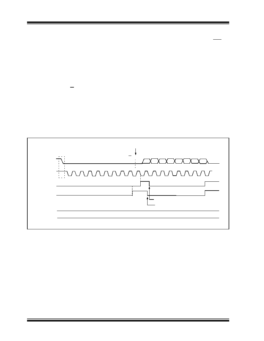
FIGURE 16-15:
SLAVE MODE GENERAL CALL ADDRESS SEQUENCE
(7 OR 10-BIT ADDRESS MODE)
SDA
SCL
S
SSPIF
BF (SSPSTAT<0>)
SSPOV (SSPCON1<6>)
Cleared in software
SSPBUF is read
R/W = 0
ACK
General Call Address
Address is compared to General Call Address
GCEN (SSPCON2<7>)
Receiving data
ACK
12
3
4
5
6
7
8
9
1
2
3
4
5
67
8
9
D7
D6
D5
D4
D3
D2
D1
D0
after ACK, set interrupt
'0'
'1'
发布紧急采购,3分钟左右您将得到回复。
相关PDF资料
PIC18F8525-E/PT
IC PIC MCU FLASH 24KX16 80TQFP
XF2L-3035-1
CONN FPC 30POS 0.5MM SMT
PIC16F1938-I/SS
IC MCU 8BIT FLASH 28SSOP
PIC16F627A-I/SO
IC MCU FLASH 1KX14 EEPROM 18SOIC
PIC18F65J11-I/PT
IC PIC MCU FLASH 16KX16 64TQFP
PIC18F2439-E/SO
IC PIC MCU FLASH 6KX16 28SOIC
PIC16LF1938-I/SS
IC MCU 8BIT FLASH 28SSOP
PIC16C621A-20/SO
IC MCU OTP 1KX14 COMP 18SOIC
相关代理商/技术参数
PIC18F4539-I/ML
功能描述:8位微控制器 -MCU 24KB 1408 RAM 32 I/O RoHS:否 制造商:Silicon Labs 核心:8051 处理器系列:C8051F39x 数据总线宽度:8 bit 最大时钟频率:50 MHz 程序存储器大小:16 KB 数据 RAM 大小:1 KB 片上 ADC:Yes 工作电源电压:1.8 V to 3.6 V 工作温度范围:- 40 C to + 105 C 封装 / 箱体:QFN-20 安装风格:SMD/SMT
PIC18F4539-I/P
功能描述:8位微控制器 -MCU 24KB 1408 RAM 32 I/O RoHS:否 制造商:Silicon Labs 核心:8051 处理器系列:C8051F39x 数据总线宽度:8 bit 最大时钟频率:50 MHz 程序存储器大小:16 KB 数据 RAM 大小:1 KB 片上 ADC:Yes 工作电源电压:1.8 V to 3.6 V 工作温度范围:- 40 C to + 105 C 封装 / 箱体:QFN-20 安装风格:SMD/SMT
PIC18F4539-I/P
制造商:Microchip Technology Inc 功能描述:IC 8BIT FLASH MCU 18F4539 DIP40
PIC18F4539-I/PT
功能描述:8位微控制器 -MCU 24KB 1408 RAM 32 I/O RoHS:否 制造商:Silicon Labs 核心:8051 处理器系列:C8051F39x 数据总线宽度:8 bit 最大时钟频率:50 MHz 程序存储器大小:16 KB 数据 RAM 大小:1 KB 片上 ADC:Yes 工作电源电压:1.8 V to 3.6 V 工作温度范围:- 40 C to + 105 C 封装 / 箱体:QFN-20 安装风格:SMD/SMT
PIC18F4539IPT
制造商:MICRO CHIP 功能描述:NEW
PIC18F4539T-E/ML
功能描述:8位微控制器 -MCU 24KB 1408 RAM 32 I/O RoHS:否 制造商:Silicon Labs 核心:8051 处理器系列:C8051F39x 数据总线宽度:8 bit 最大时钟频率:50 MHz 程序存储器大小:16 KB 数据 RAM 大小:1 KB 片上 ADC:Yes 工作电源电压:1.8 V to 3.6 V 工作温度范围:- 40 C to + 105 C 封装 / 箱体:QFN-20 安装风格:SMD/SMT
PIC18F4539T-E/PT
功能描述:8位微控制器 -MCU 24KB 1408 RAM 32 I/O RoHS:否 制造商:Silicon Labs 核心:8051 处理器系列:C8051F39x 数据总线宽度:8 bit 最大时钟频率:50 MHz 程序存储器大小:16 KB 数据 RAM 大小:1 KB 片上 ADC:Yes 工作电源电压:1.8 V to 3.6 V 工作温度范围:- 40 C to + 105 C 封装 / 箱体:QFN-20 安装风格:SMD/SMT
PIC18F4539T-I/ML
功能描述:8位微控制器 -MCU 24KB 1408 RAM 32 I/O RoHS:否 制造商:Silicon Labs 核心:8051 处理器系列:C8051F39x 数据总线宽度:8 bit 最大时钟频率:50 MHz 程序存储器大小:16 KB 数据 RAM 大小:1 KB 片上 ADC:Yes 工作电源电压:1.8 V to 3.6 V 工作温度范围:- 40 C to + 105 C 封装 / 箱体:QFN-20 安装风格:SMD/SMT